


The Future of Chipmaking: China’s LDP Lithography and the End of U.S. Sanctions?
The End of ASML’s Monopoly? China’s LDP Lithography Targets Mass Production

TL;DR:
China’s Semiconductor Breakthrough: Huawei and SMIC are developing Localized Dynamic Patterning (LDP) lithography, a potential alternative to ASML's EUV technology. Targeting trial production in Q3 2025 and full-scale rollout by 2026.
ASML's Monopoly & U.S. Sanctions: ASML remains the sole supplier of EUV machines, with critical components sourced from the U.S., Germany, and Japan. U.S. export bans since 2019 have blocked China from obtaining this technology, forcing domestic R&D efforts.
Why EUV Matters: Sub-5nm chips require EUV’s single-patterning precision. Without it, China relies on multi-patterning DUV, which is inefficient, costly, and limits yield. Essential for AI, 5G, HPC, and military applications.
China’s Workaround – LDP Lithography: Instead of ASML’s laser-produced plasma (LPP) EUV, LDP may use a different method (e.g., alternative light sources or plasma generation). Key challenges include matching EUV precision, overcoming sanctions on key materials, and achieving industrial scalability.
Economic & Geopolitical Impact: A successful LDP rollout could reduce China’s reliance on foreign semiconductor technology, weaken U.S. sanctions, and intensify competition with TSMC & Samsung. The U.S. may escalate sanctions or increase domestic chip investments.
Future Outlook: While progress is promising, full self-sufficiency remains uncertain. China still lacks critical foreign-sourced components, and mass-producing high-yield sub-5nm chips is a major hurdle. The semiconductor tech war is far from over.
And now for the Deep Dive….
Introduction
The semiconductor industry is foundational to modern technology, underpinning advancements in computing, telecommunications, and various electronic devices. Central to semiconductor fabrication is lithography, a process that transfers intricate circuit patterns onto silicon wafers. As device dimensions shrink to enhance performance and energy efficiency, lithography techniques have evolved, with extreme ultraviolet (EUV) lithography emerging as a pivotal technology for producing sub-5nm chips. This evolution has intensified the technological rivalry between the United States and China, leading to strategic sanctions aimed at curbing China's access to cutting-edge semiconductor manufacturing tools.
The dominance of ASML, a Dutch company, in the EUV lithography market is a testament to the complexity and precision required in modern chip fabrication. ASML's EUV machines utilize a 13.5nm wavelength light source, enabling the printing of minuscule features essential for advanced semiconductors. These systems are indispensable for leading chip manufacturers like TSMC and Samsung. The geopolitical significance of such technology has led to U.S.-led export controls, effectively restricting ASML from supplying EUV equipment to Chinese firms, thereby impeding China's progression in high-end chip manufacturing.
In response to these constraints, Chinese companies such as Huawei and Semiconductor Manufacturing International Corporation (SMIC) have accelerated their research and development efforts to achieve self-reliance in semiconductor fabrication. A notable development is their reported advancement in localized dynamic patterning (LDP) lithography, a potential alternative to traditional EUV techniques. This breakthrough aims to circumvent existing technological barriers and sanctions, with trial productions anticipated in the third quarter of 2025 and full-scale manufacturing by 2026. If successful, this innovation could significantly bolster China's semiconductor industry, reducing its dependence on foreign technology and altering the global semiconductor landscape.
 on X: \"China is out competing ASML. The laser-induced discharge plasma (LDP) EUV generation commercialization push is a DeepSeek moment for lithography that I was fearful of. LDP is")
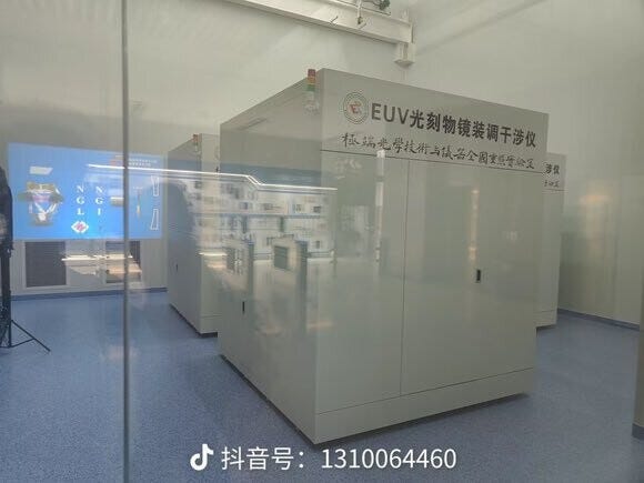
(Pictured above: Schematic of how localized dynamic patterning (LDP) lithography is set up)
Understanding EUV Lithography
Extreme Ultraviolet (EUV) lithography is an advanced photolithographic technique that utilizes light with a wavelength of approximately 13.5 nanometers to pattern extremely fine features on semiconductor wafers. This short wavelength allows for the fabrication of semiconductor devices with feature sizes smaller than 5 nanometers, enabling higher transistor densities and improved performance. Due to the high absorption of EUV light by most materials, traditional refractive optics like lenses are unsuitable; instead, EUV systems employ highly reflective mirrors coated with multilayer materials to direct and focus the light onto the wafer.
The adoption of EUV lithography is crucial for advancing chip manufacturing technologies, as it facilitates the production of smaller, faster, and more energy-efficient semiconductor devices. By enabling high-density transistor placement, EUV lithography enhances computational performance and reduces power consumption, which is essential for applications in artificial intelligence, 5G communications, and high-performance computing. Compared to Deep Ultraviolet (DUV) lithography, which operates at a wavelength of approximately 193 nanometers and often requires multiple patterning steps to achieve similar resolutions, EUV lithography simplifies the patterning process for sub-7nm features, thereby increasing yield and manufacturing efficiency.
The transition from DUV to EUV lithography represents a significant technological advancement in semiconductor fabrication. While DUV lithography relies on longer wavelengths and necessitates complex multiple patterning techniques to achieve fine resolutions, EUV's shorter wavelength allows for single-exposure patterning of smaller features, reducing process complexity and cost. However, EUV lithography presents its own set of challenges, including the need for vacuum environments due to the high absorption of EUV light by air, the development of novel photoresists compatible with EUV wavelengths, and the requirement for defect-free reflective masks. Despite these challenges, the superior resolution capabilities of EUV lithography make it indispensable for the continued scaling of semiconductor devices in accordance with Moore's Law.

ASML's Dominance in EUV Technology
ASML Holding N.V., a Dutch multinational corporation, has established itself as the sole supplier of extreme ultraviolet (EUV) lithography machines, which are indispensable for fabricating advanced semiconductor devices with feature sizes below 5 nanometers. Each EUV system, priced at approximately $200 million, is a culmination of intricate engineering and collaboration with specialized suppliers across the globe. The production of these machines involves critical components sourced from leading technology firms in the United States, Germany, and Japan, underscoring the collaborative nature of this high-tech industry.
The technological sophistication of ASML's EUV machines presents significant barriers to entry for potential competitors. A pivotal component is the precision optics developed by Carl Zeiss AG in Germany, which manufactures mirrors with atomic-scale accuracy to effectively reflect and focus EUV light. Additionally, the high-powered carbon dioxide (CO₂) lasers, essential for generating the EUV light source, are produced by Cymer, a subsidiary of ASML based in the United States. The requirement for ultra-high vacuum environments and the integration of complex subsystems further contribute to the formidable engineering challenges, making the replication of ASML's technology exceedingly difficult.
ASML's exclusive capability to produce EUV lithography systems has profound implications for the global semiconductor market. The company supplies these advanced tools to a select group of leading chip manufacturers, including Taiwan Semiconductor Manufacturing Company (TSMC), Samsung Electronics, and Intel Corporation. This exclusivity means that regions or companies without access to ASML's EUV technology face significant limitations in advancing their semiconductor fabrication processes, particularly at the most advanced nodes. Consequently, countries like China, which are currently restricted from acquiring ASML's EUV machines due to export controls, encounter substantial challenges in developing cutting-edge semiconductor manufacturing capabilities.
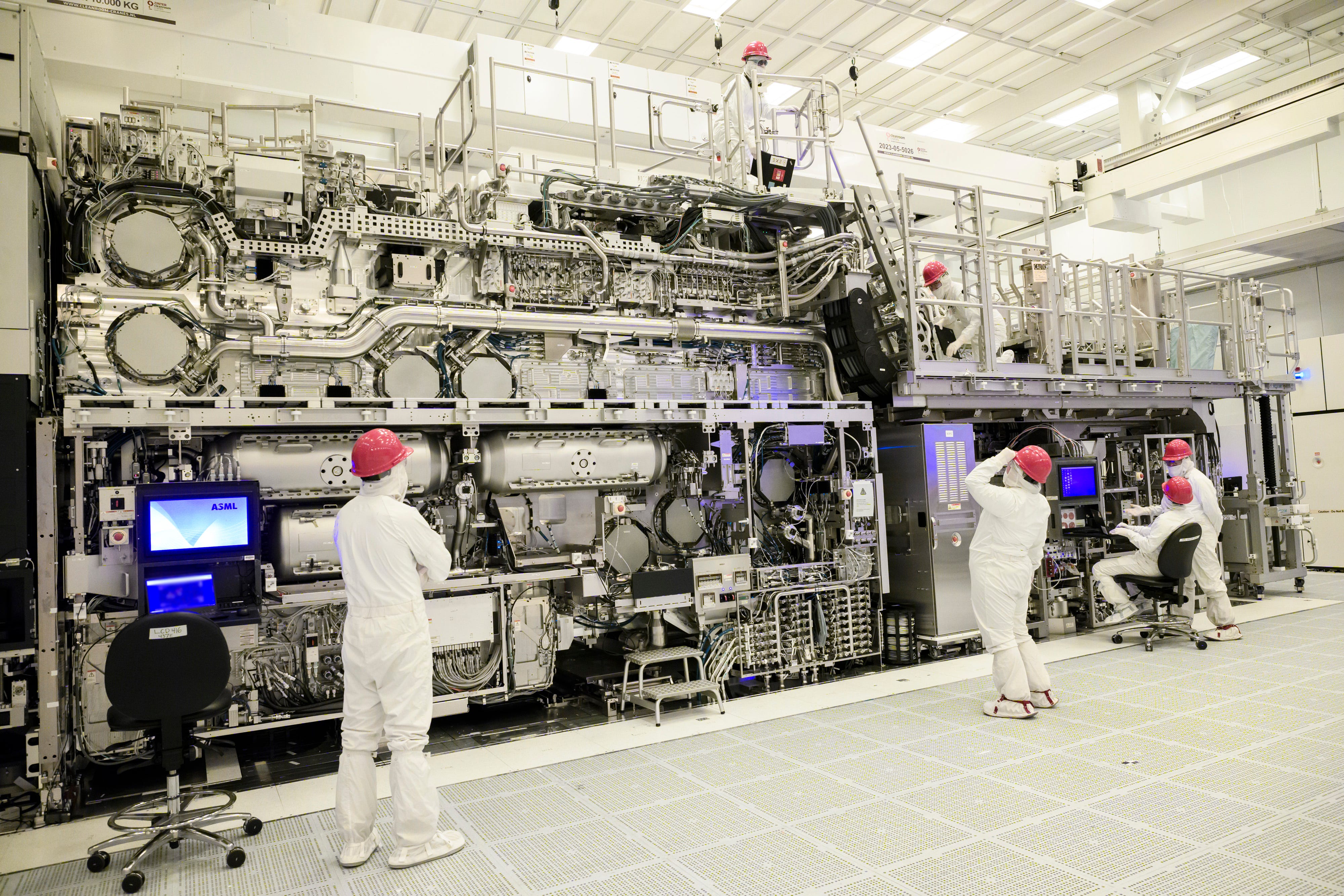
(Pictured above: Part of the EUV machine)
U.S.-Led Sanctions Against EUV Export to China
The United States has implemented stringent export controls to curtail China's access to advanced semiconductor manufacturing technologies, particularly targeting companies like Huawei and Semiconductor Manufacturing International Corporation (SMIC). In October 2022, the U.S. Department of Commerce's Bureau of Industry and Security (BIS) introduced comprehensive measures restricting China's ability to procure and develop advanced computing and semiconductor manufacturing items. These controls encompass limitations on exporting advanced chips and semiconductor manufacturing equipment to China, aiming to impede the nation's technological advancements in sectors deemed critical to U.S. national security and foreign policy interests.
These export controls have significantly impacted China's semiconductor industry, compelling companies like SMIC to rely on older deep ultraviolet (DUV) lithography technologies. Without access to extreme ultraviolet (EUV) lithography equipment, essential for producing cutting-edge chips, Chinese manufacturers have resorted to multi-patterning techniques using DUV systems to achieve finer feature sizes. This approach, however, introduces increased complexity, higher production costs, and reduced efficiency, hindering China's competitiveness in the global semiconductor market. Consequently, there is an intensified focus within China on achieving self-reliance through domestic innovation and technological breakthroughs in lithography and other critical semiconductor fabrication processes.
The broader implications of these U.S.-led sanctions extend beyond immediate operational challenges for Chinese semiconductor firms. The restrictions have disrupted global supply chains, as companies worldwide reassess their dependencies and strategies in response to the evolving geopolitical landscape. Notably, the U.S. CHIPS and Science Act, a $52 billion federal initiative, aims to revitalize domestic semiconductor manufacturing and research, reducing reliance on foreign suppliers and enhancing national security. This legislation underscores a strategic shift towards bolstering domestic capabilities in response to China's ambitions in the semiconductor sector, reflecting the intricate interplay between policy, technology, and global economic dynamics.
The Role of EUV in Sub-5nm Chip Production
Extreme ultraviolet (EUV) lithography has become indispensable for fabricating semiconductor devices at sub-5nm technology nodes, primarily due to its ability to achieve single-patterning precision essential for such advanced scaling. The utilization of 13.5 nm wavelength light in EUV lithography facilitates the creation of extremely fine features on silicon wafers, thereby enabling the production of high-density, high-performance integrated circuits. In contrast, reliance on deep ultraviolet (DUV) lithography for these nodes necessitates complex multi-patterning techniques to achieve similar resolutions. These additional patterning steps not only introduce increased process complexity but also elevate production costs and potentially reduce overall yield, making EUV lithography the preferred method for efficient and precise manufacturing at these advanced scales.
The application of EUV lithography extends across a spectrum of cutting-edge technologies, including artificial intelligence (AI), quantum computing, and advanced smartphones, all of which demand high-performance and energy-efficient chips. Moreover, EUV's capability to produce densely packed transistors is critical for military and national security applications that require robust high-performance computing solutions. The strategic importance of mastering EUV technology is underscored by its potential to confer a significant competitive advantage in the semiconductor industry, influencing global technological leadership and economic power.
China's current status in advanced chip manufacturing reflects both progress and challenges. Notably, Semiconductor Manufacturing International Corporation (SMIC) has achieved a 7nm process node using DUV-based multi-patterning techniques, as evidenced by the production of Huawei's Kirin 9000S chip. However, the absence of EUV lithography poses significant hurdles for SMIC in scaling down to 5nm and beyond, as the reliance on multi-patterning not only increases manufacturing complexity but also impacts yield and cost-effectiveness. This technological gap underscores the critical need for China to develop indigenous EUV capabilities to remain competitive in the rapidly evolving semiconductor landscape.

China’s EUV Breakthrough: LDP Lithography
China's semiconductor industry has been actively pursuing advancements in lithography technology to circumvent restrictions on acquiring extreme ultraviolet (EUV) lithography equipment from leading suppliers like ASML. A notable development in this endeavor is the reported progress by Huawei and Semiconductor Manufacturing International Corporation (SMIC) in developing Localized Dynamic Patterning (LDP) lithography. This innovative approach is being positioned as a potential alternative to traditional EUV systems, with trial production anticipated in the third quarter of 2025 and mass production targeted for 2026.
LDP lithography distinguishes itself from conventional EUV techniques through its unique method of generating the requisite 13.5 nm wavelength light. Specifically, LDP employs a process that involves vaporizing tin between electrodes and converting it into plasma via high-voltage discharge. This plasma generation method produces the necessary EUV radiation, offering several technical advantages over the laser-produced plasma (LPP) technique utilized by ASML. The LDP approach potentially simplifies system architecture, reduces the equipment footprint, enhances energy efficiency, and lowers production costs, marking a significant departure from existing EUV methodologies.
Despite these promising developments, several critical challenges must be addressed to bring LDP lithography to fruition. Securing the necessary materials and components under current international sanctions poses a significant hurdle, as access to advanced technologies and equipment is restricted. Additionally, achieving high yield rates and minimizing defects are paramount to ensure the commercial viability of chips produced using LDP lithography. Furthermore, refining the LDP tools to match the precision and throughput of established EUV systems is essential for competitiveness. Scaling these tools for industrial-level production also presents a formidable challenge that requires substantial investment and technical expertise.
The potential success of LDP lithography carries significant implications for the global semiconductor industry. By developing a domestic alternative to ASML's EUV machines, China could mitigate the impact of export controls and reduce its reliance on foreign technology for advanced chip manufacturing. This advancement would not only bolster China's position in the semiconductor supply chain but also challenge the existing monopoly held by ASML in the EUV market. Such a shift could lead to increased competition, potentially driving innovation and reducing costs in the industry.
However, it is important to note that while the LDP lithography approach shows promise, the path to widespread adoption is fraught with technical and logistical challenges. The development timeline, from trial production to mass production, is ambitious and contingent upon overcoming significant obstacles. The global semiconductor community will be closely monitoring China's progress in this area, as successful implementation of LDP lithography could reshape the dynamics of semiconductor manufacturing and influence global technology policies.

Implications of China’s Breakthrough
China's recent advancements in localized dynamic patterning (LDP) lithography, spearheaded by industry leaders such as Huawei and Semiconductor Manufacturing International Corporation (SMIC), signify a pivotal move towards reducing dependence on foreign semiconductor technologies. By developing indigenous lithography solutions, China aims to achieve greater self-sufficiency in semiconductor manufacturing, thereby mitigating the impact of U.S. export controls designed to restrict access to advanced chip-making equipment. This strategic shift not only challenges the efficacy of existing sanctions but also underscores China's commitment to bolstering its domestic technological capabilities.
The successful implementation of LDP lithography could precipitate significant economic and geopolitical shifts within the global semiconductor supply chain. China's ability to produce advanced semiconductors domestically would introduce a formidable competitor to established industry giants such as Taiwan Semiconductor Manufacturing Company (TSMC) and South Korea's Samsung. This heightened competition could lead to market share redistribution and influence global pricing structures. In response, the United States may consider intensifying sanctions or augmenting investments in domestic semiconductor research and development to maintain its technological edge.
The evolution of China's LDP lithography initiative is poised to significantly influence the trajectory of the U.S.-China technological rivalry. Should China overcome the technical challenges associated with LDP lithography and achieve mass production, the United States might implement additional export restrictions to curtail China's access to complementary technologies and materials. Furthermore, key players in the semiconductor equipment industry, including ASML, as well as nations like Japan and members of the European Union, may reassess their export policies and collaborative engagements with China to align with shifting geopolitical dynamics.
In anticipation of China's potential technological advancements, the United States and its allies may escalate investments in their domestic semiconductor industries. Initiatives such as the U.S. CHIPS and Science Act, which allocates substantial funding to revitalize domestic chip manufacturing, exemplify strategic efforts to reduce reliance on foreign semiconductor sources. Additionally, fostering international collaborations among allied nations could serve as a countermeasure to China's growing influence in the semiconductor sector, ensuring a diversified and resilient global supply chain.
In conclusion, China's progress in developing LDP lithography represents a critical juncture in the global semiconductor landscape. The potential reduction in dependence on foreign technology, coupled with the ensuing economic and geopolitical ramifications, underscores the need for strategic responses from global industry stakeholders. As the U.S.-China tech rivalry intensifies, the actions taken by both nations and their allies will profoundly shape the future of semiconductor innovation and supply chain dynamics.
Conclusion
China's recent advancements in semiconductor technology, particularly through companies like Huawei and SMIC, signify a pivotal shift towards technological self-reliance. Despite facing stringent U.S. export controls aimed at curbing access to advanced chip-making equipment, these companies have made notable progress. For instance, Huawei has improved its production yield of advanced AI chips to nearly 40%, up from 20% the previous year, marking a significant step towards China's goal of self-sufficiency in advanced chip production.
In the short term, this breakthrough could lead to a realignment of global semiconductor supply chains, challenging the dominance of established industry leaders such as Taiwan's TSMC and South Korea's Samsung. The emergence of competitive Chinese semiconductor manufacturers may prompt these companies to innovate more rapidly and adjust pricing strategies to maintain their market positions. Concurrently, the United States might respond by implementing stricter export controls or increasing investments in domestic semiconductor research and development to preserve its technological edge.
Looking ahead, China's pursuit of self-sufficiency in chip manufacturing faces both opportunities and challenges. While significant investments and policy initiatives, such as the "Made in China 2025" plan, have been directed towards reducing reliance on foreign technology, achieving complete autonomy in semiconductor production remains complex. Critical components and advanced manufacturing equipment are still predominantly sourced from foreign suppliers, necessitating continued efforts in domestic innovation and international collaboration. The success of these endeavors will significantly influence China's position in the global technology landscape and its ability to mitigate external technological dependencies.
Sources:
Nover, S. (2024, August 20). The most powerful company in tech is a niche Dutch business you've never heard of. Retrieved from https://www.sherwoodnews.com/technology/asml-dominance-in-euv-lithography
Shilov, A. (2024, October 8). TSMC's EUV N7+ node hits volume production. Retrieved from https://www.technews.com/tsmc-euv-n7-plus-production
Tarasov, K. (2022, March 23). ASML is the only company making the $200 million machines needed to print every advanced microchip. Here's an inside look. Retrieved from https://www.techinsider.com/asml-euv-machines-inside-look
Trueman, C. (2024, November 1). TSMC to receive first High NA EUV lithography machine from ASML in Q4. Retrieved from https://www.datacenterdynamics.com/en/news/tsmc-high-na-euv-machine-asml-q4-2024
Extreme ultraviolet lithography. (2025). Wikipedia. Retrieved from https://en.wikipedia.org/wiki/Extreme_ultraviolet_lithography
ASML Holding. (2025). Wikipedia. Retrieved from https://en.wikipedia.org/wiki/ASML_Holding
Multiple patterning. (2025). Wikipedia. Retrieved from https://en.wikipedia.org/wiki/Multiple_patterning
5 nm process. (2025). Wikipedia. Retrieved from https://en.wikipedia.org/wiki/5_nm_process
Kynge, J. (2024, November 19). Transcript: The geopolitics of chips: A manufacturing miracle. Financial Times. Retrieved from https://www.ft.com/content/ae1b2088-47d9-4890-8da8-f0838b708cbc
Tarasov, K. (2022, March 23). ASML is the only company making the $200 million machines needed to print every advanced microchip. Here's an inside look. CNBC. Retrieved from https://www.cnbc.com/2022/03/23/asml-the-only-company-making-the-200-million-extreme-ultraviolet-lithography-machines.html
Clark, D. (2021, July 4). The tech cold war's 'most complicated machine' that's out of China's reach. The New York Times. Retrieved from https://www.nytimes.com/2021/07/04/technology/tech-cold-war-chips.html
Trueman, C. (2024, November 1). TSMC to receive first High NA EUV lithography machine from ASML in Q4. Data Center Dynamics. Retrieved from https://www.datacenterdynamics.com/en/news/tsmc-to-receive-first-high-na-euv-lithography-machine-from-asml-in-q4/
Bureau of Industry and Security. (2022, October 7). Commerce Implements New Export Controls on Advanced Computing and Semiconductor Manufacturing Items to the People's Republic of China (PRC). Retrieved from https://www.bis.doc.gov/index.php/documents/about-bis/newsroom/press-releases/3126-2022-10-07-bis-press-release-advanced-computing-and-semiconductor-manufacturing-controls-final/file
Reuters. (2025, February 12). China's purchases of chipmaking equipment to decline in 2025, consultancy says. Retrieved from https://www.reuters.com/technology/chinas-purchases-chipmaking-equipment-decline-2025-consultancy-says-2025-02-12/
Klein, J. (2025, February 28). A journey through the hyper-political world of microchips. The Guardian. Retrieved from https://www.theguardian.com/technology/2025/feb/28/inside-the-mind-bending-tin-blasting-and-hyper-political-world-of-microchips
Rulison, L. (2025, January 15). CHIPS Act: The tech moon shot already happening in our backyard. Times Union. Retrieved from https://www.timesunion.com/business/article/chips-tech-moonshot-already-happening-backyard-19986640.php
Nellis, S. (2023, September 6). US lawmaker calls for ending Huawei, SMIC exports after chip breakthrough. Reuters. Retrieved from https://www.reuters.com/technology/us-lawmaker-calls-ending-huawei-smic-exports-after-chip-breakthrough-2023-09-06/
Kynge, J. (2024, November 19). Transcript: The geopolitics of chips: A manufacturing miracle. Financial Times. Retrieved from https://www.ft.com/content/ae1b2088-47d9-4890-8da8-f0838b708cbc
Clark, D. (2021, July 4). The tech cold war's 'most complicated machine' that's out of China's reach. The New York Times. Retrieved from https://www.nytimes.com/2021/07/04/technology/tech-cold-war-chips.html
Trueman, C. (2024, November 1). TSMC to receive first High NA EUV lithography machine from ASML in Q4. Data Center Dynamics. Retrieved from https://www.datacenterdynamics.com/en/news/tsmc-to-receive-first-high-na-euv-lithography-machine-from-asml-in-q4/
Li, L. (2025, March 11). China's EUV breakthrough: Huawei, SMIC reportedly advancing LDP lithography, eye 3Q25 trial, 2026 rollout. DIGITIMES Asia. Retrieved from https://www.digitimes.com/news/a20250311VL200/euv-huawei-smic-2026-production.html
Shilov, A. (2025, March 8). China develops domestic EUV tool, ASML monopoly in trouble. TechPowerUp. Retrieved from https://www.techpowerup.com/333801/china-develops-domestic-euv-tool-asml-monopoly-in-trouble
South China Morning Post. (2025, February 15). How China's award-winning EUV breakthrough sidesteps US chip ban. Retrieved from https://www.scmp.com/news/china/science/article/3295209/how-chinas-award-winning-euv-breakthrough-sidesteps-us-chip-ban
TrendForce. (2025, March 10). China’s homegrown EUV machines rumored for Q3 trial production, spelling trouble for ASML. Retrieved from https://www.trendforce.com/news/2025/03/10/news-chinas-homegrown-euv-machines-rumored-for-q3-trial-production-spelling-trouble-for-asml/
Kynge, J. (2024, November 19). The US has spurred the Chinese chip industry. Financial Times. Retrieved from https://www.ft.com/content/9ffa18c4-1ef9-4801-ba6d-9058c67f3b40
Clark, D. (2021, July 4). The tech cold war's 'most complicated machine' that's out of China's reach. The New York Times. Retrieved from https://www.nytimes.com/2021/07/04/technology/tech-cold-war-chips.html
Nellis, S. (2023, September 6). US lawmaker calls for ending Huawei, SMIC exports after chip breakthrough. Reuters. Retrieved from https://www.reuters.com/technology/us-lawmaker-calls-ending-huawei-smic-exports-after-chip-breakthrough-2023-09-06/
Shilov, A. (2024, February 6). China's chipmaker SMIC on track to produce sanctions-busting 5nm processors for Huawei this year: Report. Tom's Hardware. Retrieved from https://www.tomshardware.com/news/chinas-chipmaker-smic-on-track-to-produce-sanctions-busting-5nm-processors-for-huawei-this-year-report
Kynge, J. (2024, November 19). The US has spurred the Chinese chip industry. Financial Times. Retrieved from https://www.ft.com/content/9ffa18c4-1ef9-4801-ba6d-9058c67f3b40
Nellis, S. (2023, September 6). US lawmaker calls for ending Huawei, SMIC exports after chip breakthrough. Reuters. Retrieved from https://www.reuters.com/technology/us-lawmaker-calls-ending-huawei-smic-exports-after-chip-breakthrough-2023-09-06/
Allen, G. (2023, October 6). In Chip Race, China Gives Huawei the Steering Wheel: Huawei's New Smartphone and the Future of Semiconductor Export Controls. Center for Strategic and International Studies. Retrieved from https://www.csis.org/analysis/chip-race-china-gives-huawei-steering-wheel-huaweis-new-smartphone-and-future-semiconductor
Shilov, A. (2024, February 6). China's chipmaker SMIC on track to produce sanctions-busting 5nm processors for Huawei this year: Report. Tom's Hardware. Retrieved from https://www.tomshardware.com/news/chinas-chipmaker-smic-on-track-to-produce-sanctions-busting-5nm-processors-for-huawei-this-year-report